
Trying to figure out this display, that I acquired. No real plans for it. Just thought that it was pretty cool. The only thing I have going so far is the electroluminescent (EL) backlight.
Just using this to keep notes, as I learn more about it. Also open to suggestions and clues.
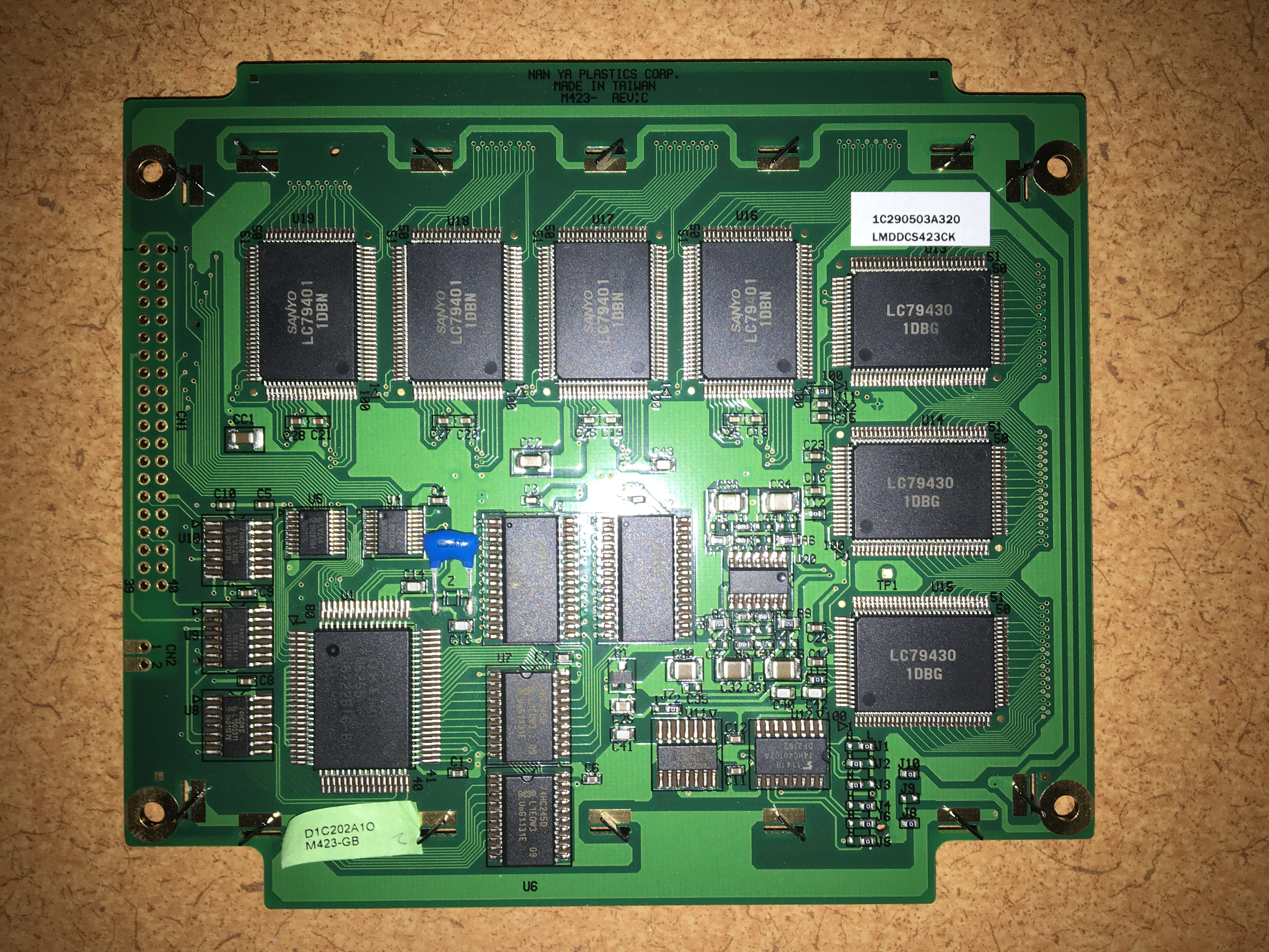
Numbers on white sticker:- 1C290503A320
- LMDDCS423C
Details on Board:
- (1) 2 pin power connector for EL backlight
- (2) 40 Pin Connector
- (1) OKI M6255 (MSM6255) Dot Matrix LCD Controller
- (4) Sanyo LC79401 Dot-Matrix LCD Drivers
- (3) Sanyo LC79430 Dot-Matrix LCD Drivers
- (2) MT62C256F-70LL
- (2) 74HC245D CMOS OCTAL BUS TRANSCEIVER
Possible Board details on 40 PIN Connector:
- Pin 09: Power 5V or 3.3V?
- Pin 10: Power 5V or 3.3V?
- Pin 11: Ground
- Pin 12: Ground
Board details about MSM625:
White sticker with the following text:
- D1C202A1O
- M423-GB
Memory Address inputs:
- A0 is...
- A1-A15 (Memory Address inputs) are all tied together, and held low.
- DB0-DB7 (Data Bus) all feed into 74HC245D.
Board details about LCD Drivers:
The combination of the LC79401 & LC79430 tells me that it is possibly 320x240 pixels.
Pictures:
Front:

Back:
Powered EL:

References:
Had some of the pins stuffed on the previous post, reason for the delete.
ReplyDeleteThat display board is in the DRB-III scan tool, and correct it is a 320 x 240. If you know where another one can be picked up or ever want to sell that one please let me know. I've been tinkering a bit with the one in my DRB-III, and have a few more of the connector pinouts for you, but getting everything 100% would require taking one apart a bit more. I plan to put the Logic Analyzer on there and see how the DRB-III 'talks' to it, then will take a stab at getting something on the screen without it.
1 - MA7 (MA0 ~ MA14 thru U4 and U5 to U1)
2 - MA14
3 - MA8
4 - MA13
5 - MA9
6 - MA12
7 - MA10
8 - MA11
9 - 5v?
10 - 5v?
11 - GND
12 - GND
13 -
14 - MA6
15 - MA0 (Also A0 of U1, goes thru 2 Inverters of U8 first)
16 - MA5
17 - MA1
18 - MA4
19 - MA2
20 - MA3
21 - DB6 (DB0 ~ DB7 go thru U6 to U1 and U7)
22 - DB7
23 - DB4
24 - DB5
25 - DB2
26 - DB3
27 - DB0
28 - DB1
29 - Goes to U10p4 (Part of the ~CE circuit for U3)
30 -
31 -
32 -
33 -
34 -
35 -
36 - BUSY (From U1, goes thru U8 first)
37 -
38 -
39 -
40 -
Thank you for the information.
ReplyDeleteYou trying to fix your DRB-III Scan Tool, or something?
I might be able to sell mine, or get my hands on another one.
I'd like to eventually do something with it. If I can remember where I obtained it, I will let you know.
Welcome, and Thanks.
ReplyDeleteI have her apart to sort out a dead line on the screen that's been on my nerves for awhile, and I just decided since it's all apart I'll just schematic up the LCD board for the snot of it.
Updated pinout with some more added and corrections.
1 - MA7 (MA0 ~ MA14 thru U4 and U5 to U1)
2 - MA14
3 - MA8
4 - MA13
5 - MA9
6 - MA12
7 - MA10
8 - MA11
9 - 5v
10 - 5v
11 - GND
12 - GND
13 - ~WR
14 - MA6
15 - MA0 (Also A0 of U1, goes thru 2 Inverters of U8 first)
16 - MA5
17 - MA1
18 - MA4
19 - MA2
20 - MA3
21 - DB6 (DB0 ~ DB7 go thru U6 to U1 and U7)
22 - DB7
23 - DB4
24 - DB5
25 - DB2
26 - DB3
27 - DB0
28 - DB1
29 - Goes to U10p4 (Part of the ~CE circuit for U3)
30 - Goes to U10p9 (Part of the ~CE circuit for U2)
31 -
32 - BUSY (From U1, goes thru U8 first)
33 - Goes to U9p13 (Part of the DIR circuit for U6 and U7)
34 - ~CS (Thru U10, as buffer)
35 - Q1 Base (Contrast Control?)
36 - VE (To Q1c, Q1e goes to LCD driver VEE pins)
37 -
38 -
39 -
40 -
I've found what I also consider to be a hardware bug on the board. U9p14 (VCC) is not connected to anything, except C9. That pin should be going to the 5v rail on the board, and it does not. I've been over that thing multiple times looking for where it was getting 4.4v from, and it just goes nowhere. Finally dawned on me that the chip is getting power via the steering diodes of it's Input lines. It still 'works' that way, but really should be corrected, and was interesting to find that problem in there after decades.
Without being able to tear into the PCB (effectively destroying it in the process) to be able to verify everything, this is about as close as I can get for now on a schematic of that board. None of the Capacitor values are in there, but none are critical values anyway, and I'm not about to go tearing into my working board here given what these things still cost when you run across them.
ReplyDeletehttps://www.acidmods.com/RDC/DRB-III/DRB-III_LCD_Schematic_NAN_YA_LMDDCS423CK.pdf
Thank you for sharing that. If get my hands on another after the holidays, I will let you know. Traveling for work, mixed with the holidays, made December tight.
ReplyDeleteIf I come up short, I would also probably be willing to unload mine, considering you have more use for it, to fix your DRB-III scanner.
Welcome.
ReplyDeleteSchematic has been updated a bit, mostly just housekeeping things. Also have a PCB made up to be able to tap the Scope and Logic Analyzer onto there with everything running normally to 'see' what is going on.
The power supply requirement for that thing is +5v and -24v, then the Contrast control line also needs a negative voltage on it for adjusting that. The DRB-III can adjust that from around -17v to -21v, and you can just use a 10k TRIMPOT as a voltage divider from -24v to Ground to get that voltage and be able to adjust it where it looks best.
Pinouts updated a bit now also after going over the schematic a bit. (may change again when the Scope/LA gets on them)
LMDDCS243CK (see schematic for details)
CN1
1 - MA7
2 - MA14
3 - MA8
4 - MA13
5 - MA9
6 - MA12
7 - MA10
8 - MA11
9 - 5v
10 - 5v
11 - GND
12 - GND
13 - ~WR
14 - MA6
15 - MA0/AD0
16 - MA5
17 - MA1
18 - MA4
19 - MA2
20 - MA3
21 - DB6
22 - DB7
23 - DB4
24 - DB5
25 - DB2
26 - DB3
27 - DB0
28 - DB1
29 - SRAM ~CE_U3
30 - SRAM ~CE_U2
31 - ?
32 - BUSY
33 - DIR
34 - LCD CONTROLLER ~CS
35 - CONTRAST
36 - VE, -24v
37 - ?
38 - ?
39 - ?
40 - ?
? = Currently unknown, but believe to be NC, Not Connected
CN2 - BACKLIGHT, 80vac RMS, 400Hz
Had a quick look with the Logic Analyzer at what the DRB-III does at power up with the LCD. This looking at all of the Data, Address and various Control lines the LCD uses, and is just the first 5 or so seconds after it's powered on.
ReplyDeletehttps://www.acidmods.com/RDC/DRB-III/1_Power_up_first_5_seconds.jpg
Quite a bit to process there, but not all of it is relevant to the LCD just yet. Just the parts where the ~CS trace goes LO (aka where it's setting up the LCD Controller registers) is where the LCD things start.
https://www.acidmods.com/RDC/DRB-III/2_Config_Zoom.jpg
Weeding out the traces we don't need yet, and this is the thing setting up 6 of the Registers of the MSM6255
https://www.acidmods.com/RDC/DRB-III/3_Essential.jpg
Zooming in to the very first one, the MOR Register, the fist ~CS and ~WR 'event' with MA0/AD0 = 1 is the MOR Instruction, 00000000, then the second one with MA0/AD0 = 0 is the MOR Register Data, 00001011
https://www.acidmods.com/RDC/DRB-III/4_MOR_ZOOM.jpg
Comparing that to the Datasheet, the Data for MOR setup as 00001011 means it's 32 frames, Cursor Off, Display ON, 4-bit Parallel Graphics Mode.
The other 5 Register values all jive with how the thing is setup hardware wise also.
00000001 = PR
00000111 = 7
00000010 = HNR
00100111 = 39
00000011 = DVR
11101111 = 239
00000101 = SLR
00000000 = 0
00000110 = SUR
00000000 = 0
After that, there's a mountain of data that gets loaded into the LCD RAM that will take awhile to sort all out.
RDC,
DeleteI have another board. I can ship it to you. How do you want to do it? Put it on ebay, and let you bid on it? Just give me your address (or vice versa) to figure it out. I can just give it to you, if you pay shipping.